- 您现在的位置:买卖IC网 > Sheet目录3871 > PIC18F83J11T-I/PT (Microchip Technology)IC PIC MCU FLASH 4KX16 80TQFP
PIC18F85J11 FAMILY
DS39774D-page 170
2010 Microchip Technology Inc.
16.1
CCP Module Configuration
Each Capture/Compare/PWM module is associated
with a control register (generically, CCPxCON) and a
data register (CCPRx). The data register, in turn, is
comprised of two 8-bit registers: CCPRxL (low byte)
and CCPRxH (high byte). All registers are both
readable and writable.
16.1.1
CCP MODULES AND TIMER
RESOURCES
The CCP modules utilize Timers 1, 2 or 3, depending
on the mode selected. Timer1 and Timer3 are available
to modules in Capture or Compare mode, while Timer2
is available for modules in PWM mode.
TABLE 16-1:
CCPx MODE – TIMER
RESOURCE
The assignment of a particular timer to a module is
determined by the timer to CCPx enable bits in the
T3CON register (Register 15-1). Both modules may be
active at any given time and may share the same timer
resource if they are configured to operate in the same
mode (Capture/Compare or PWM) at the same time.
The interactions between the two modules are
summarized in Table 16-2.
Depending on the configuration selected, up to four
timers may be active at once, with modules in the same
configuration (Capture/Compare or PWM) sharing
timer resources. The possible configurations are
shown in Figure 16-1.
16.1.2
OPEN-DRAIN OUTPUT OPTION
When operating in Output mode (i.e., in Compare or
PWM modes), the drivers for the CCPx pins can be
optionally configured as open-drain outputs. This
feature allows the voltage level on the pin to be pulled
to a higher level through an external pull-up resistor
and allows the output to communicate with external
circuits without the need for additional level shifters.
The open-drain output option is controlled by the
CCP2OD and CCP1OD bits (TRISG<6:5>). Setting the
appropriate bit configures the pin for the corresponding
module for open-drain operation.
16.1.3
CCP2 PIN ASSIGNMENT
The pin assignment for CCP2 (Capture input, Compare
and PWM output) can change, based on device config-
uration. The CCP2MX Configuration bit determines
which pin CCP2 is multiplexed to. By default, it is
assigned to RC1 (CCP2MX = 1). If the Configuration bit
is cleared, CCP2 is multiplexed with RE7.
Changing the pin assignment of CCP2 does not
automatically change any requirements for configuring
the port pin. Users must always verify that the appropri-
ate TRIS register is configured correctly for CCP2
operation, regardless of where it is located.
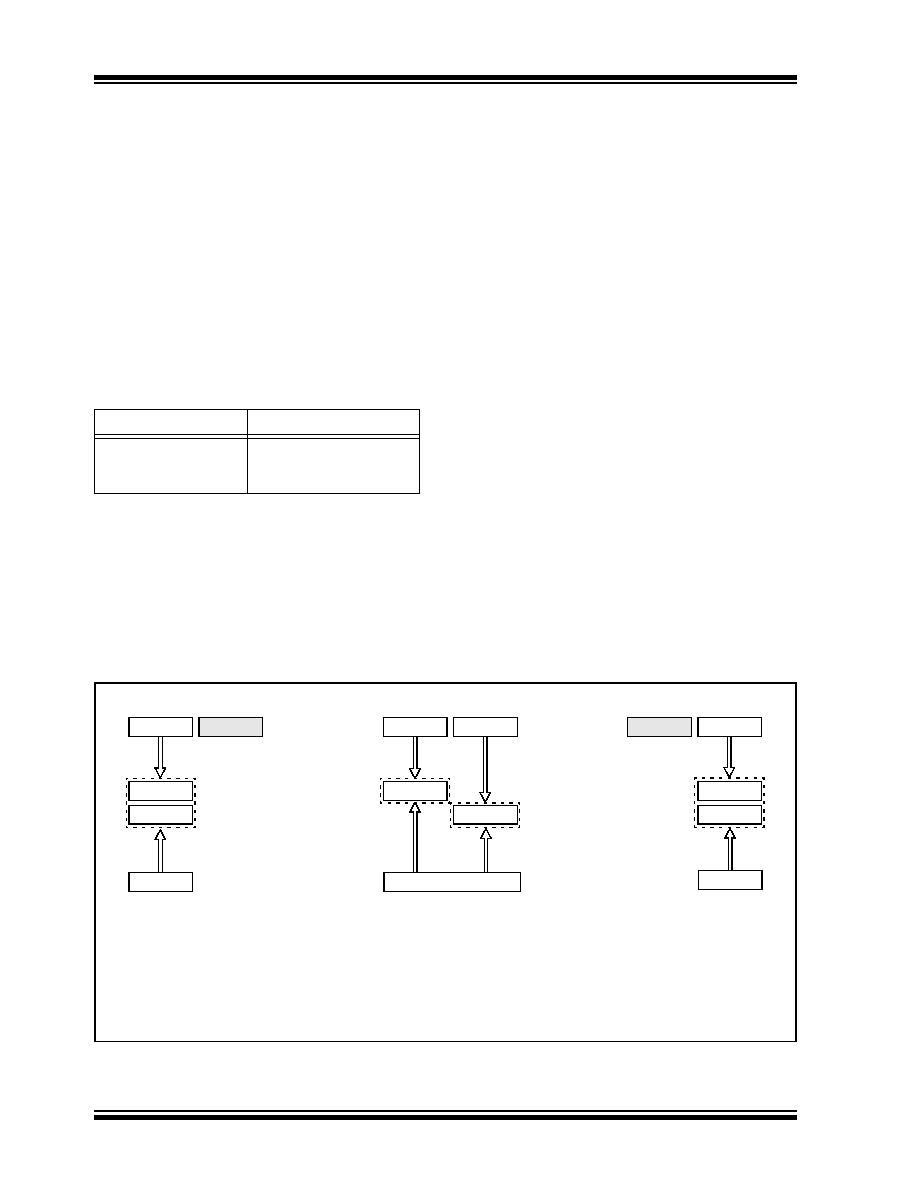
FIGURE 16-1:
CCPx AND TIMER INTERCONNECT CONFIGURATIONS
CCPx Mode
Timer Resource
Capture
Compare
PWM
Timer1 or Timer3
Timer2
TMR1
TMR2
TMR3
CCP2
CCP1
TMR1
TMR2
TMR3
CCP2
CCP1
TMR1
TMR3
TMR2
CCP2
CCP1
T3CCP<2:1> = 00
T3CCP<2:1> = 01
T3CCP<2:1> = 1x
Timer1 is used for all Capture
and Compare operations for
all CCP modules. Timer2 is
used for PWM operations for
all CCP modules. Modules
may
share
either
timer
resource as a common time
base.
Timer1 is used for Capture
and Compare operations for
CCP1 and Timer 3 is used for
CCP2.
Both the modules use Timer2
as a common time base if they
are in PWM modes.
Timer3 is used for all Capture
and Compare operations for
all CCP modules. Timer2 is
used for PWM operations for
all CCP modules. Modules
may
share
either
timer
resource as a common time
base.
发布紧急采购,3分钟左右您将得到回复。
相关PDF资料
PIC16LF627-04/P
IC MCU FLASH 1KX14 COMP 18DIP
PIC18F86J55T-I/PT
IC PIC MCU FLASH 48KX16 80TQFP
PIC18F43K22-I/MV
MCU PIC 8KB FLASH 40QFN
PIC16C55A-04I/P
IC MCU OTP 512X12 28DIP
PIC18LF43K22-I/MV
MCU PIC 8KB FLASH 40UQFN
PIC16C622A-20I/P
IC MCU OTP 2KX14 COMP 18DIP
PIC18F84J11T-I/PT
IC PIC MCU FLASH 8KX16 80TQFP
PIC18F24K22-I/SP
IC PIC MCU 16KB FLASH 28SPDIP
相关代理商/技术参数
PIC18F83J90-I/PT
功能描述:8位微控制器 -MCU 8KB FL 1024b RAM 67I/O 8b Fam RoHS:否 制造商:Silicon Labs 核心:8051 处理器系列:C8051F39x 数据总线宽度:8 bit 最大时钟频率:50 MHz 程序存储器大小:16 KB 数据 RAM 大小:1 KB 片上 ADC:Yes 工作电源电压:1.8 V to 3.6 V 工作温度范围:- 40 C to + 105 C 封装 / 箱体:QFN-20 安装风格:SMD/SMT
PIC18F83J90T-I/PT
功能描述:8位微控制器 -MCU 8KB Flash 1024bytes-RAM 67I/O RoHS:否 制造商:Silicon Labs 核心:8051 处理器系列:C8051F39x 数据总线宽度:8 bit 最大时钟频率:50 MHz 程序存储器大小:16 KB 数据 RAM 大小:1 KB 片上 ADC:Yes 工作电源电压:1.8 V to 3.6 V 工作温度范围:- 40 C to + 105 C 封装 / 箱体:QFN-20 安装风格:SMD/SMT
PIC18F8410-E/PT
功能描述:8位微控制器 -MCU 16kBF 768RM 70I/O RoHS:否 制造商:Silicon Labs 核心:8051 处理器系列:C8051F39x 数据总线宽度:8 bit 最大时钟频率:50 MHz 程序存储器大小:16 KB 数据 RAM 大小:1 KB 片上 ADC:Yes 工作电源电压:1.8 V to 3.6 V 工作温度范围:- 40 C to + 105 C 封装 / 箱体:QFN-20 安装风格:SMD/SMT
PIC18F8410-I/PT
功能描述:8位微控制器 -MCU 16kBF 768RM 70I/O RoHS:否 制造商:Silicon Labs 核心:8051 处理器系列:C8051F39x 数据总线宽度:8 bit 最大时钟频率:50 MHz 程序存储器大小:16 KB 数据 RAM 大小:1 KB 片上 ADC:Yes 工作电源电压:1.8 V to 3.6 V 工作温度范围:- 40 C to + 105 C 封装 / 箱体:QFN-20 安装风格:SMD/SMT
PIC18F8410T-I/PT
功能描述:8位微控制器 -MCU 16kBF 768RM 70I/O RoHS:否 制造商:Silicon Labs 核心:8051 处理器系列:C8051F39x 数据总线宽度:8 bit 最大时钟频率:50 MHz 程序存储器大小:16 KB 数据 RAM 大小:1 KB 片上 ADC:Yes 工作电源电压:1.8 V to 3.6 V 工作温度范围:- 40 C to + 105 C 封装 / 箱体:QFN-20 安装风格:SMD/SMT
PIC18F8490-E/PT
功能描述:8位微控制器 -MCU 16kBF 768RM 66I/O RoHS:否 制造商:Silicon Labs 核心:8051 处理器系列:C8051F39x 数据总线宽度:8 bit 最大时钟频率:50 MHz 程序存储器大小:16 KB 数据 RAM 大小:1 KB 片上 ADC:Yes 工作电源电压:1.8 V to 3.6 V 工作温度范围:- 40 C to + 105 C 封装 / 箱体:QFN-20 安装风格:SMD/SMT
PIC18F8490-I/PT
功能描述:8位微控制器 -MCU 16kBF 768RM 66I/O RoHS:否 制造商:Silicon Labs 核心:8051 处理器系列:C8051F39x 数据总线宽度:8 bit 最大时钟频率:50 MHz 程序存储器大小:16 KB 数据 RAM 大小:1 KB 片上 ADC:Yes 工作电源电压:1.8 V to 3.6 V 工作温度范围:- 40 C to + 105 C 封装 / 箱体:QFN-20 安装风格:SMD/SMT
PIC18F8490-I/PT
制造商:Microchip Technology Inc 功能描述:IC 8BIT FLASH MCU 18F8490 TQFP80